Everyone has seen a circuit board - usually it's the distinctive green boards we remember. They are built into electronic devices and ensure the incredible variety of functions. That sounds banal at first. But it is not.
But what makes printed circuit boards and their processing so essential?
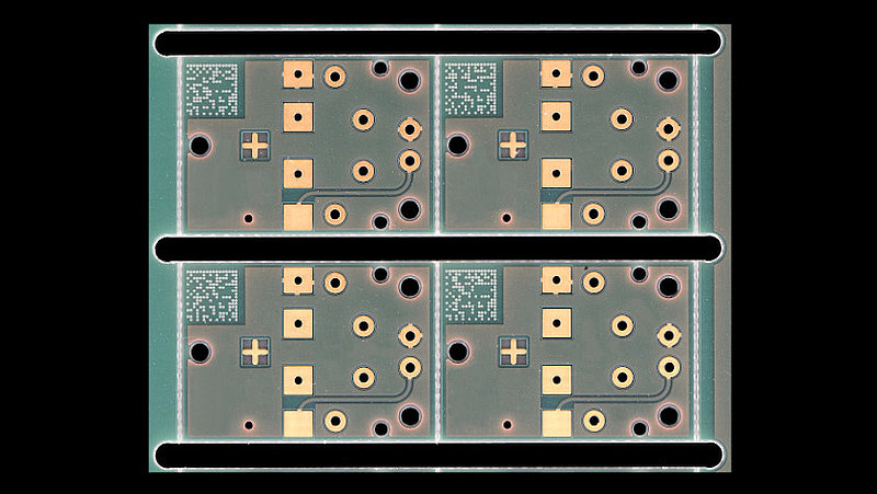
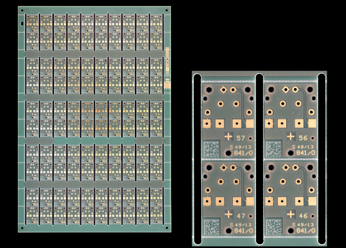
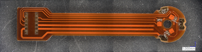
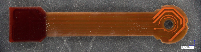
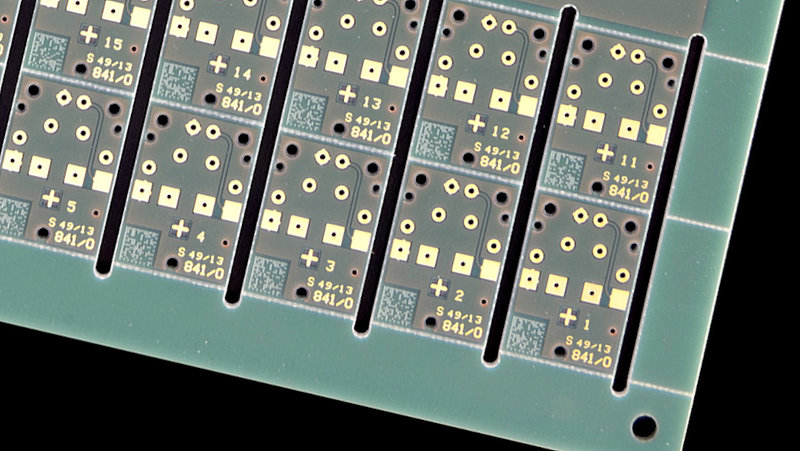
Printed circuit boards consist of electrically insulating material. Usually it is fiber-reinforced plastic with conductive connections attached to it, so-called conductor tracks. The types of boards range from single-sided printed circuit boards to multilayer and flexible forms, as well as special technologies. They are used in practically all electronic devices. In most cases, there is not only 1 printed circuit board, but several at the same time inside electrical devices - they are the heart of the respective device. Without them nothing works. For example, highly complex machines in industry, medicine, smart household appliances, automated automobiles, but also PCs, laptops and of course smartphones and as a new technology in the form of wearables. In today's world of ever-smaller devices and significantly more electronics in everyday life, this means that PCBs must be ever smaller, thinner, yet more complex and functional, as well as having long-term stability. Particularly in the latter case, technical cleanliness in the processing of the PCBs plays a very important role. This is because residues from machining processes on the circuit boards can lead to growing crystal structures and thus to short circuits or malfunctions.
How can contamination be avoided or a high level of technical cleanliness be ensured in the processing of printed circuit boards?
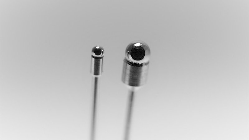
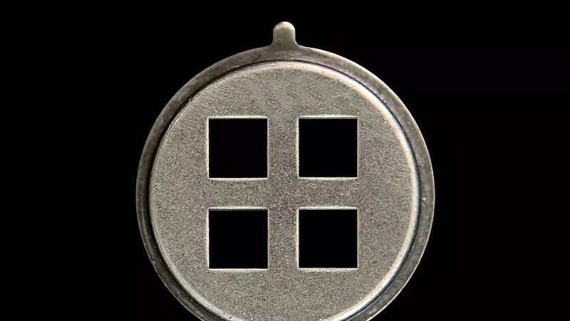
The basic requirement is the use of innovative laser cutting technology combined with experience and knowledge in the processing of different PCB materials (multilayer, flex, rigid-flex).
The technological problem:
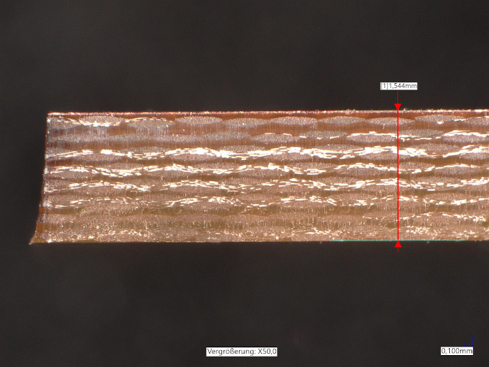
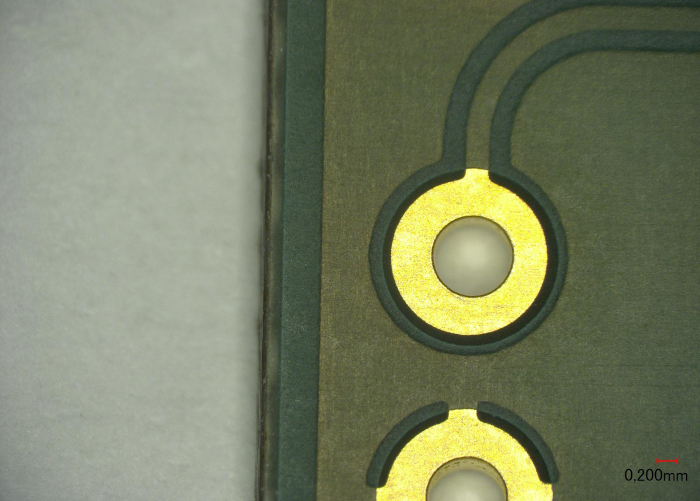
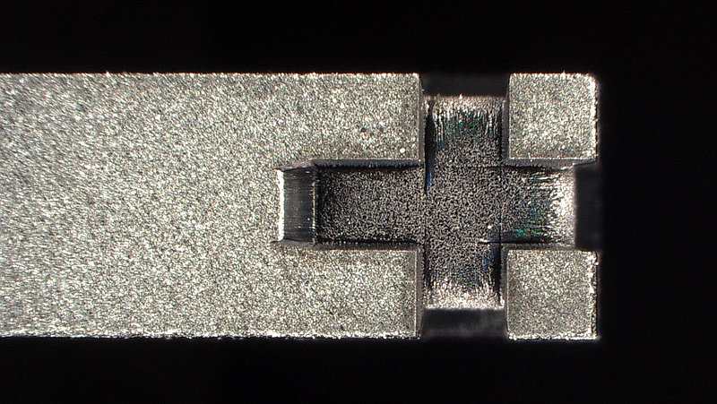
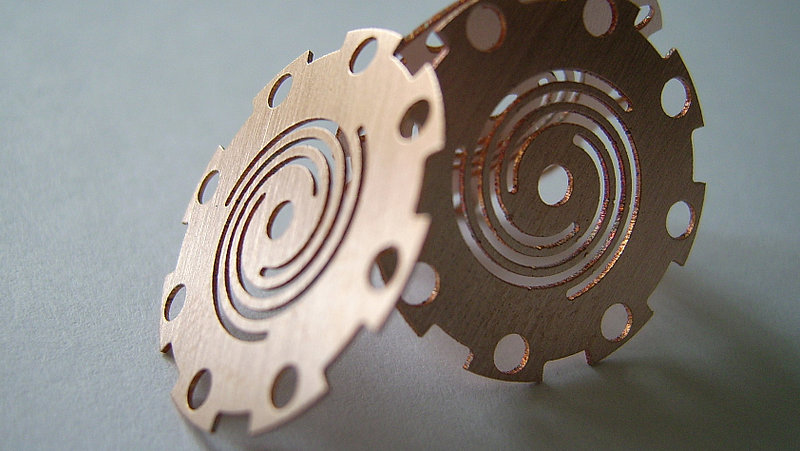
Today, laser systems are still being sold with laser depaneling processes that use technology that is more than 20 years old and thus cause carbonization during laser cutting and drilling. In this process, energy is transferred from the laser into the material and converted into heat. As a result, the material heats up, melts and immediately vaporizes. This releases carbons, which have decisive disadvantages for the user: an unpleasant smell, visual defects due to a black-colored cutting or drilling edge, and poor surface quality.
The solution:
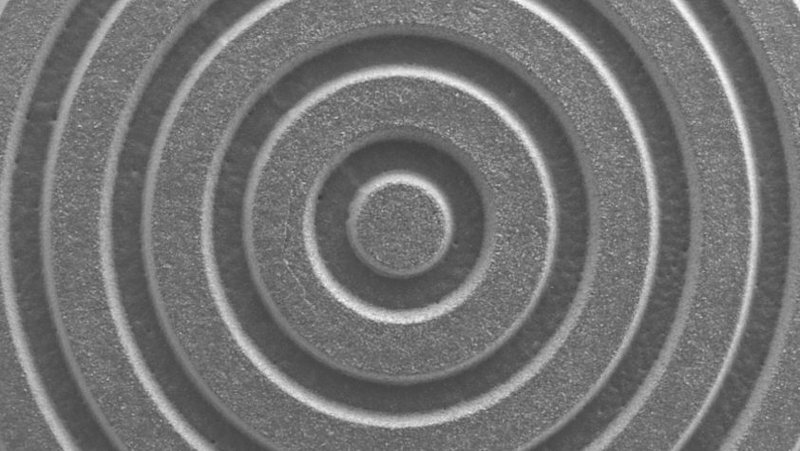
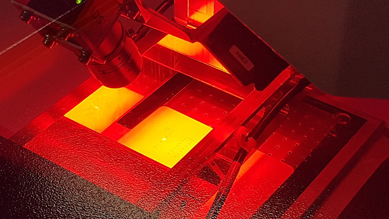
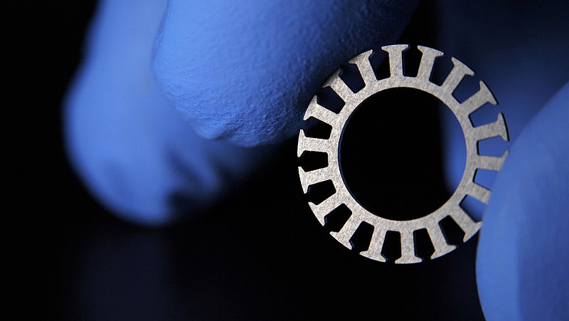
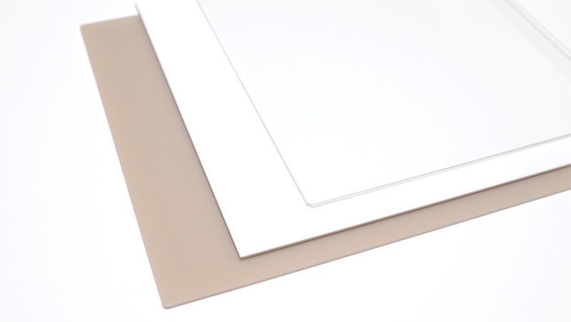
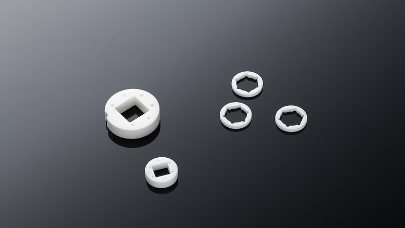
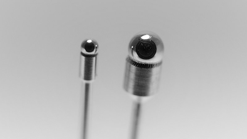
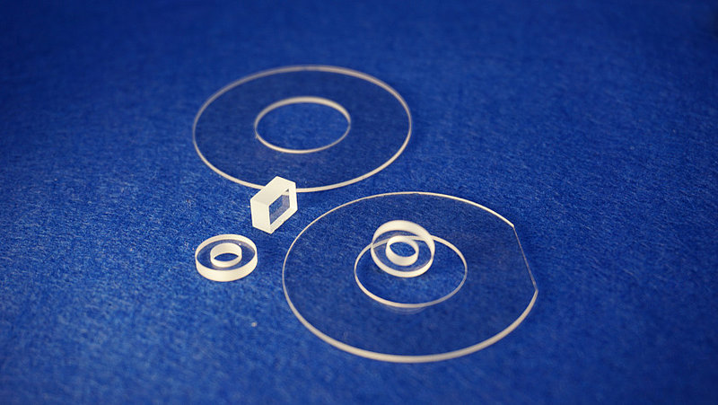
The latest generations of ultra-short pulse laser sources (USP) offer clean and stress-free cutting and drilling technology at a comparatively high processing speed. Both flexible and rigid PCBs can be processed completely without carbonization. This raises the quality of the cutting edges to a new level and also increases the reliability as well as the service life of these electronic components. The innovative laser technology enables distortion-free laser cutting of PCB contours and cover layers, laser drilling of the smallest vias, blind holes and through-holes in PCBs, laser structuring of board surfaces and, increasingly, laser cutting of thin plastic foils and screens. Furthermore, laminated, metallized or vaporized plastic foils can be processed. Laser cutting of paper and thin insulation materials are also included. All in all, the USP laser can process a wide range of different PCB materials and plastic foils - always considering that the most optimal laser parameters per material and thickness have to be selected.
The extended solution approach:
Do you have challenges in the micromachining of materials? You lack technological equipment at the latest technology level and many years of experience as well as profound know-how? You want to focus on your core competencies? Then LCP Laser-Cut-Processing GmbH is the right partner for you. The company takes over your high-end micromaterial processing of special materials using the latest laser technologies and various processing methods coupled with many years of know-how. Outsource your material processing challenges to the specialist. Thus you remain flexible and save your own cost- and maintenance-intensive plant technology, tied-up personnel resources as well as a build-up of long-standing, deep know-how. Your advantage with LCP: You receive a fast, reliable special service adapted to your individual needs, on which you can rely - from consulting and prototype production to possible series production along the entire process chain!
Please feel free to contact us!


![[Translate to English:] Silizium Wafer](/fileadmin/_processed_/4/5/csm_silizium_wafer_842_022e209b94.jpg)