Your wafers in good hands
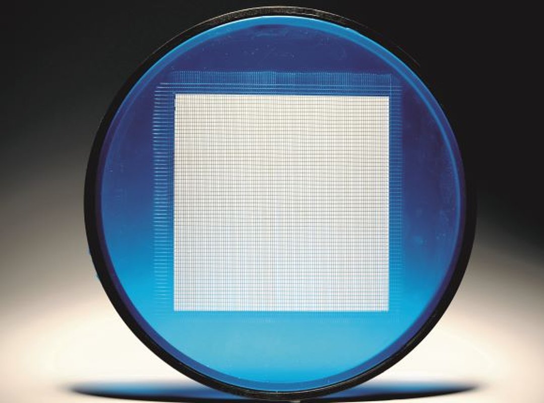
A wafer is a flat blank made of semiconductor materials such as silicon or gallium arsenide. Wafers are used in the semiconductor industry as starting material for the production of microchips and other electronic components. Wafer dicing describes the precision processing of wafers and substrates made of HTCC (high temperature co-fired ceramics) and LTCC (low temperature co-fired ceramics) such as ceramics, silicon, glass, germanium, sapphire, quartz, COB circuit boards or metal foils by means of mechanical cutting (sawing). The advantage of using the wafer saw is the extremely precise separation of the wafers, the exact edge quality and the variety of materials to be processed - including short set-up times.
Wafer processing options
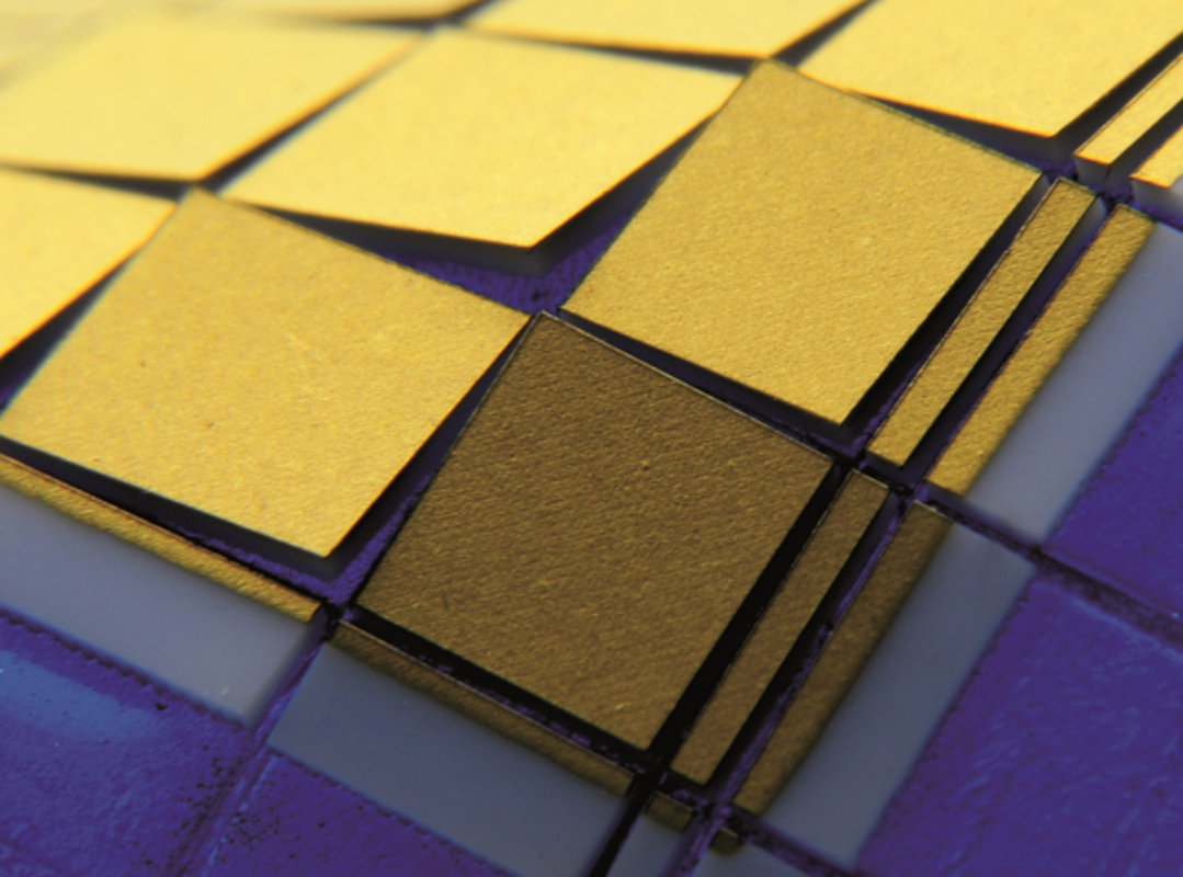
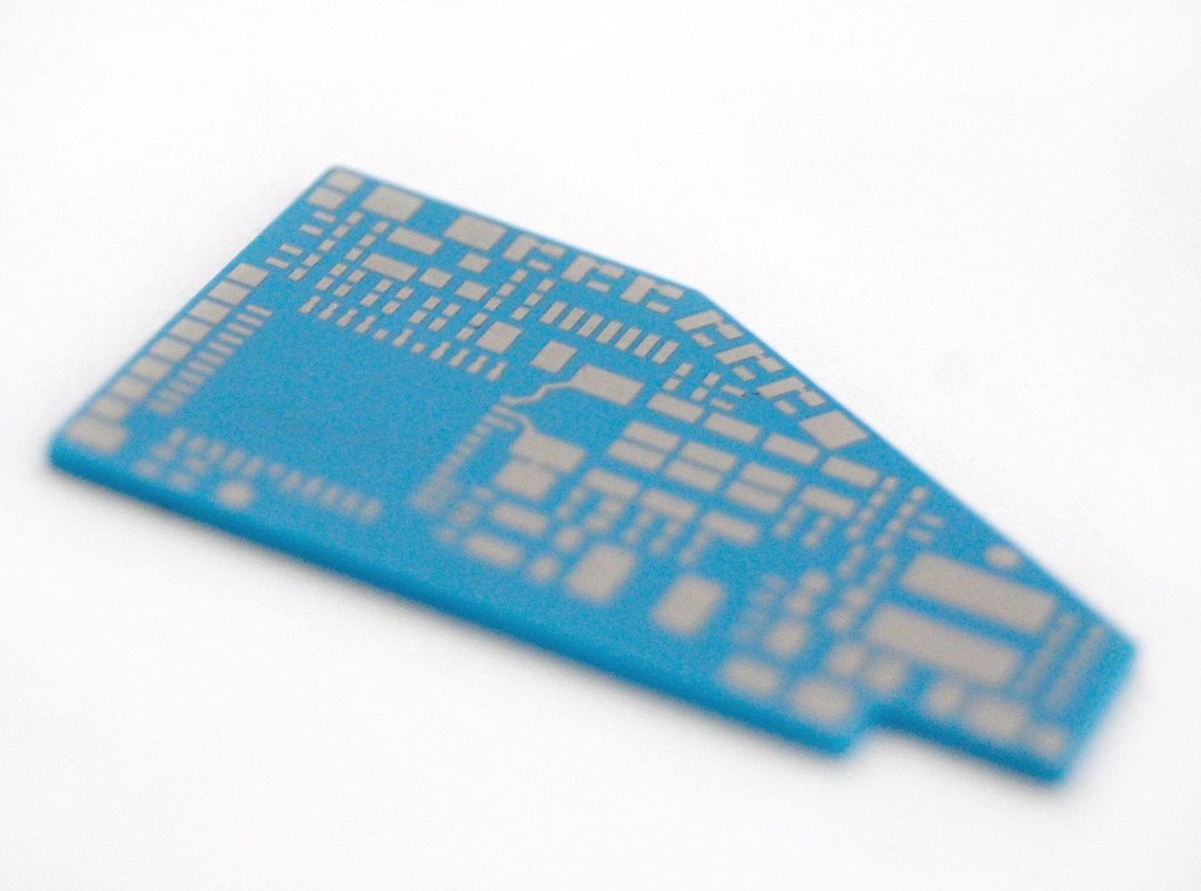
Separating wafers and substrates into individual chips is an essential step in semiconductor and microtechnology. Wafer sawing is usually performed with saw blades that are fed through the wafer along sawing or grooving lines to divide it into small chips by means of cutoff grinding, formatting or separation. Alternatively, scribe lines can be applied to the wafer surface to facilitate cutting. The choice of the appropriate sawing and cutting process and the final diameter depends on the specific requirements of the process. This requires high precision to avoid damage and material residues on the chips and to ensure full functionality of the final product.
The separated wafers and substrates can be delivered on foil left in the saw frame, in 2" or 4" waffle packs, already taped or in transport containers of your choice.
Further details can be found in our data sheets.
Typical areas of application for wafer dicing
Wafer Dicing is used for the following applications:
- grading and separating IR filter elements
- cutting of semiconductor components (optoelectronic components, LEDs)
- production of ceramic components in combination with laser processing as SMD components according to JEDEC standard
- structuring of quartz glass elements
- separation of multilayer ceramics (LTCC) in the printed state
- separation of piezoceramics for signalling or fine positioning
Wafer sawing for various products
The grinding process in wafer dicing is complex and a high-precision operation that can be used to manufacture a wide range of products. In this process, excellent edge quality is critical to ensure the functionality of the final product. We support you in the production of:
Our services for you
We process your substrates and wafers according to your specifications. Depending on the installation conditions and application purpose, a combination of laser and dicing processing can also prove useful and sensible. Our staff will be happy to advise you on this.
Discover more technologies now and take a look at our available materials.