Predetermined breaking points for depanelization
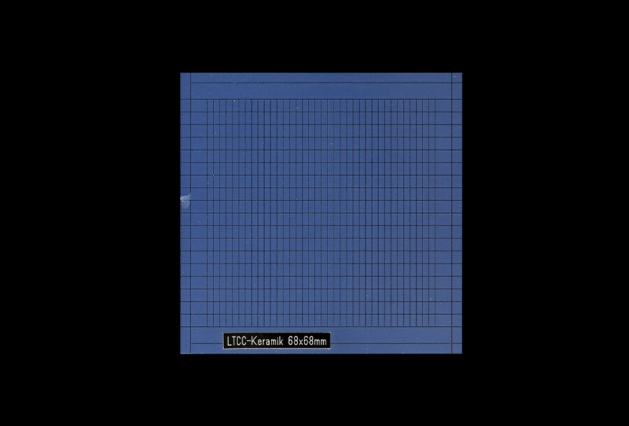
Especially when using hard-brittle materials such as ceramics made of aluminum oxide, silicon nitride or low-temperature co-fired ceramics (LTCC) for the production of circuit carriers in hybrid electronics, the production in a so-called panel arrangement, which means the arrangement of several individual circuits on a raw substrate or wafer for joint production as a batch, has proven itself.
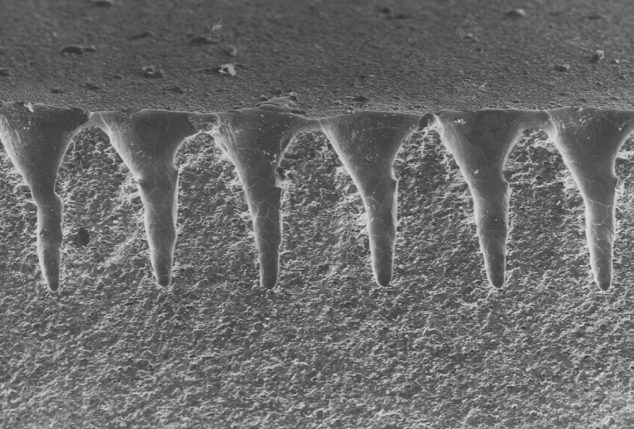
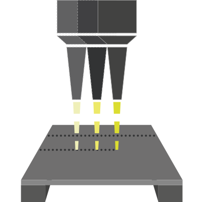
With the help of laser scribing, scribe lines are inserted on the substrate. This bullet hole or these bullet holes are visible in the form of closely spaced blind holes or notches. A blind hole is only lasered to a certain depth. This creates predetermined breaking points while avoiding a breakthrough. This weakening of the material serves as a perforation line. After the production run, breaking along these scribe lines enables the mechanical separation of the multiple panel into the individual components.
With the pearl chain-like stringing of blind holes, both the penetration depth and the spacing or overlapping of the individual blind holes can be determined. If there is a large overlap, this is referred to as the production of a notch trench, which in turn has a strong resemblance to the notch trenches introduced during the punching of unfired ceramic substrates (green state). This processing technology enables more efficient production of individual parts by means of a panel arrangement not only for ceramic materials, but also for glasses, silicon and even some metals.
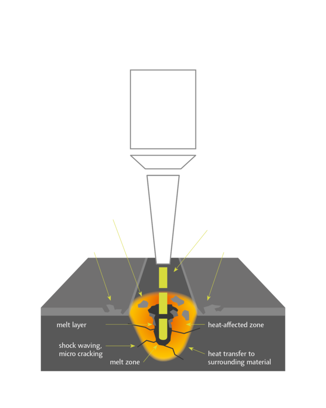

The new “NextGen” process combines efficiency, cleanliness, and yield in an optimized procedure. During “cold” ablation, no heat is introduced into the material, which prevents potential material damage and microcracks. Due to the physical effect of sublimation, the material also evaporates directly, meaning no disruptive melt residues or burrs are formed. This completely eliminates the time-consuming post-processing required by the standard process. At the same time, the significantly narrower kerf lines enable finer structuring, allowing up to 25% more usable area to be obtained from the same substrate.