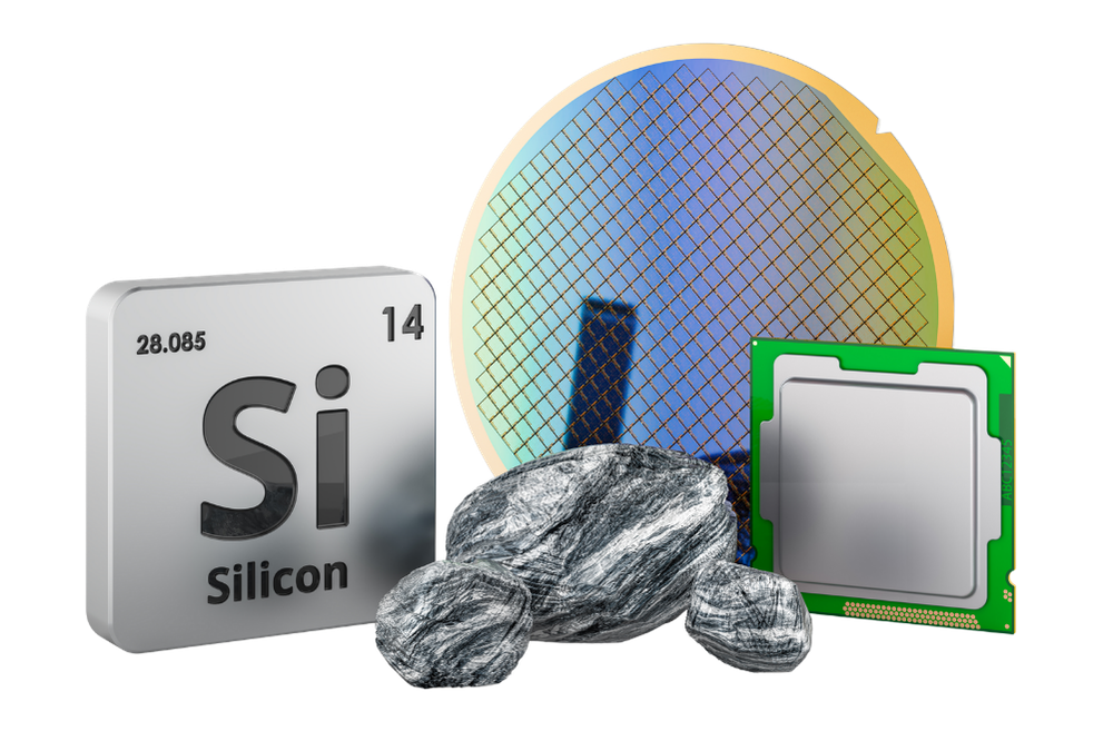
What Is Silicon? – A Key Material in Semiconductor Technology
Silicon is a semimetal and one of the most important elements in microelectronics. It combines the properties of metals and nonmetals, making it ideally suited as a semiconductor material.
It occurs in large quantities in the Earth’s crust (approximately 25.8 %) and is processed into a high-purity form for use in the semiconductor industry.
Typical applications of silicon wafers:
- microelectronics and integrated circuits (ICs)
- power electronics
- MEMS and sensor systems
- photovoltaics/solar cells

Precision Laser Processing of Silicon Wafers
Laser processing of silicon wafers requires the highest precision, as the material is brittle and must meet extremely high purity requirements. Non-contact, thermally controlled laser processes are therefore crucial for consistent results.
To this end, we use high-precision laser processing methods that are specifically designed for semiconductor and wafer processes.
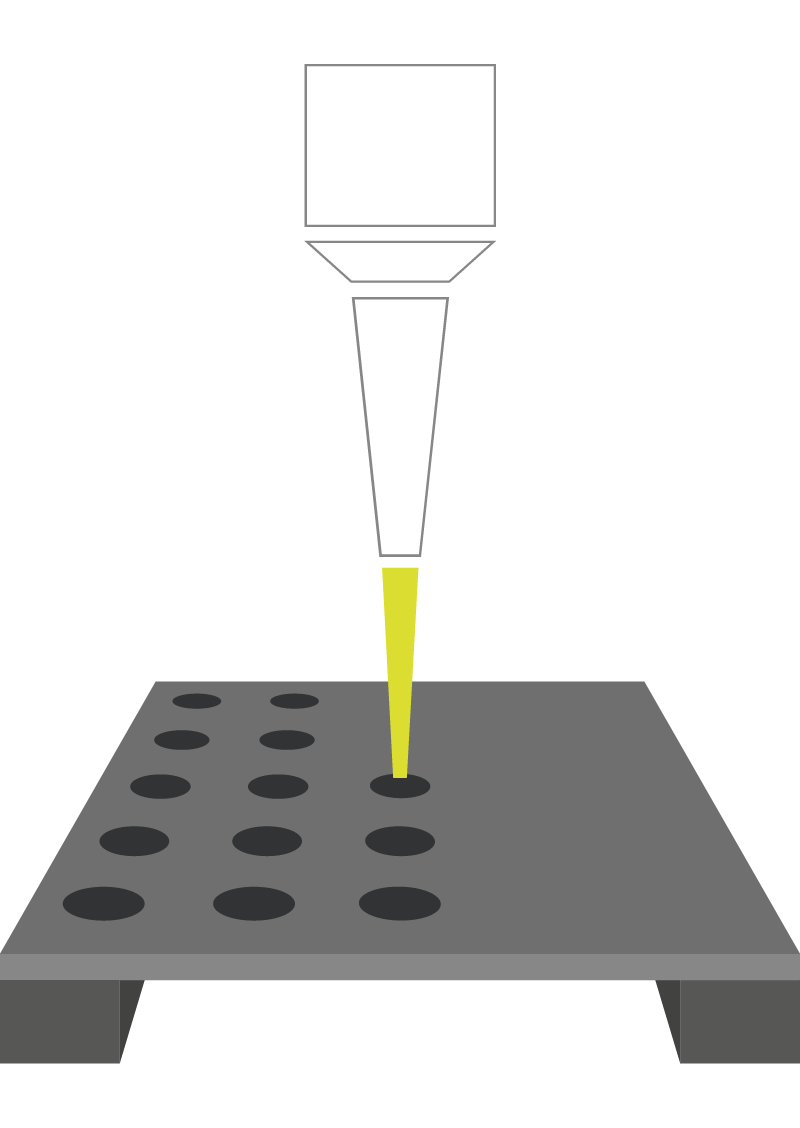
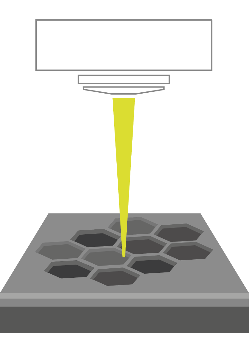
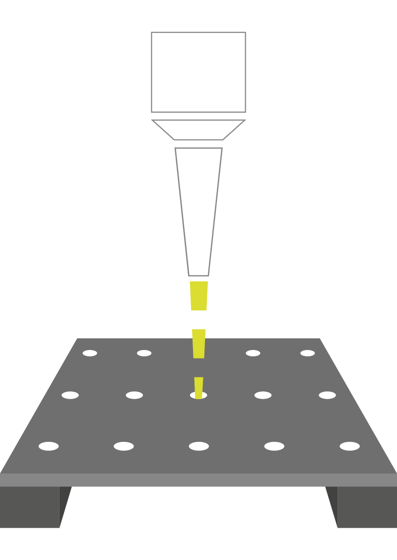
Using state-of-the-art laser technologies, we implement high-precision processing methods for silicon wafers—ranging from silicon laser cutting, laser structuring, laser drilling, and laser scribing to wafer dicing. The result is reproducible manufacturing processes, the highest precision, and excellent processing quality for demanding applications in the semiconductor and microelectronics industries.