Create functional surface structures
The purpose of laser structuring is to create simple or complex surface modifications by means of material removal, thermal interaction or precise energy input and thus to functionalize them. It is a process that is used both for roughening or smoothing hardened metallic or ceramic component surfaces for tribological improvements. The term laser structuring covers both partial and precise surface material removal, as well as large-area laser polishing, laser cleaning and laser honing. There are no limits to the type and scope of laser structuring - regardless of whether you require single or full-surface structuring of components. But it can also be used to activate specific conductive path structures in plastics or to build up layer systems. The term laser structuring covers both partial and precise surface material removal as well as large-area laser polishing, laser cleaning and laser honing.There are no limits to the type and scope of laser processing - regardless of whether you require individual or full-surface structuring of components.
In laser structuring with an ultra-short pulse laser, the material vaporizes without leaving any melt residue on the component. Thanks to so-called cold ablation, the material is not melted but vaporized, which enables high-quality structuring of the material. Ultra-short pulse lasers consequently allow cleaner and often post-processing-free microstructuring of surfaces with very high precision.
Technical possibilities of laser processing of surfaces
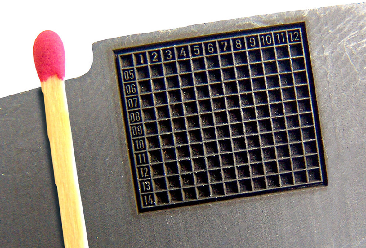
Laser systems for surface structuring, surface modification and micromachining play a crucial role in industrial manufacturing and research. The various processes such as microstructuring, microcutting, ablation, notching and layer ablation enable precise, flexible and diverse processing in the micrometer range. Both deep ablation and surface modifications are realized by ablation, decoating, polishing or roughening. Cavities and blind holes are also implemented by micromachining. A special technique used in this process are ultrashort pulse laser sources, which generate extremely short pulses in the pico-/femtosecond range. Our services support you in activating and cleaning surfaces through a wide range of processing.
Manufacturing technology for different materials
Whether thin-film wafer or thick-film substrate: surface processing by means of laser structuring is suitable for a wide range of different materials. These include metals as well as non-metals and especially hard-brittle materials. Thanks to precise manufacturing technology, the possibilities for processing the following materials are virtually unlimited:
- aluminum oxide (Al2O3, sapphire)
- aluminum nitride (AlN)
- silicon (Si) and silicon nitride (Si3N4)
- sintered silicon carbide (SSiC)
- recrystallized silicon carbide (RSiC)
- glass (-ceramic), quartz
- plastic printed circuit boards made of FR3/FR4/ FR5 (PCB)
- ceramic circuit boards or multilayer (LTCC)
Application areas of laser technology
The very high light intensities achieved in micromachining with ultrashort pulse lasers enable the processing of materials where mechanical processing or other laser technologies reach their limits. However, the advantage of laser processing also lies in the flexibility with which any shape can be produced quickly, precisely and economically.
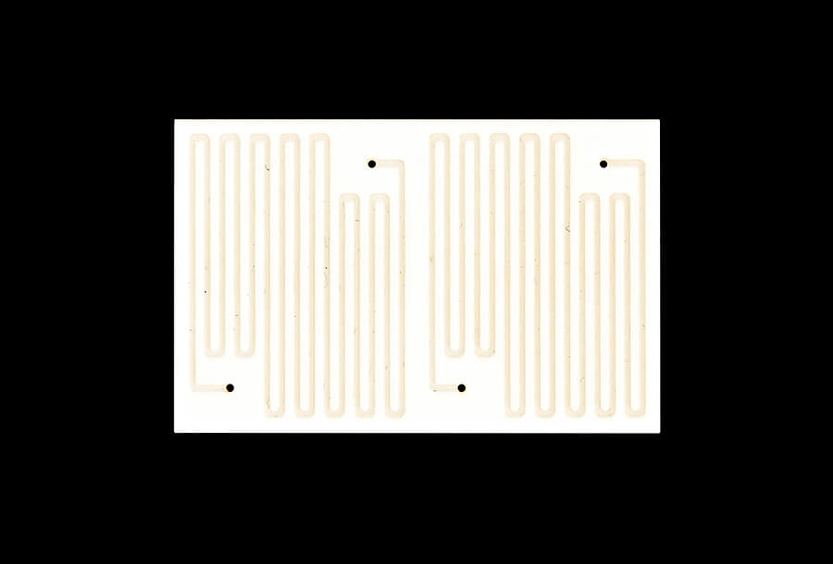
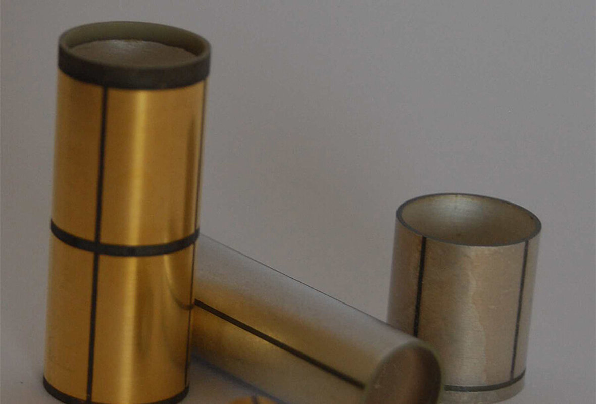
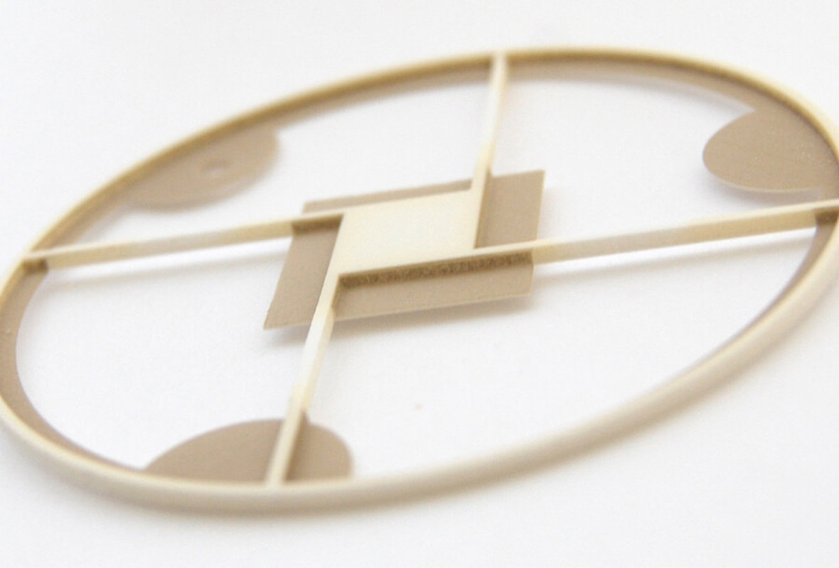
With the help of clamping devices, so-called chucks, or suction devices with negative pressure, the ultrashort pulse laser cuts materials cleanly without damaging them. Ceramics, glasses and metals are drilled, structured and cut without thermal damage to the material. This opens up new possibilities in electronics, mechanics, medical technology and microfluidics. The versatile manufacturing technology is ideal for useful and network substrates and other thick film hybrids. We support you in the fabrication of:
- heaters,
- conductors,
- masks,
- apertures,
- stencils,
- circuit carriers,
- and microreactors.
Laser processing allows surfaces in the micrometer range to be processed particularly efficiently and precisely. Particularly when using ultrashort pulse lasers, residue-free material removal is feasible, especially when materials are subsequently to be coated - for example, in metallization. For this purpose, no material residues must adhere to the substrates.
Discover our wide range of services
Our large portfolio of machining technologies enables us to produce fast, precise and individual components according to your specifications - from laser drilling and wafer dicing to precision manufacturing of drawing parts.