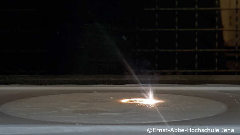
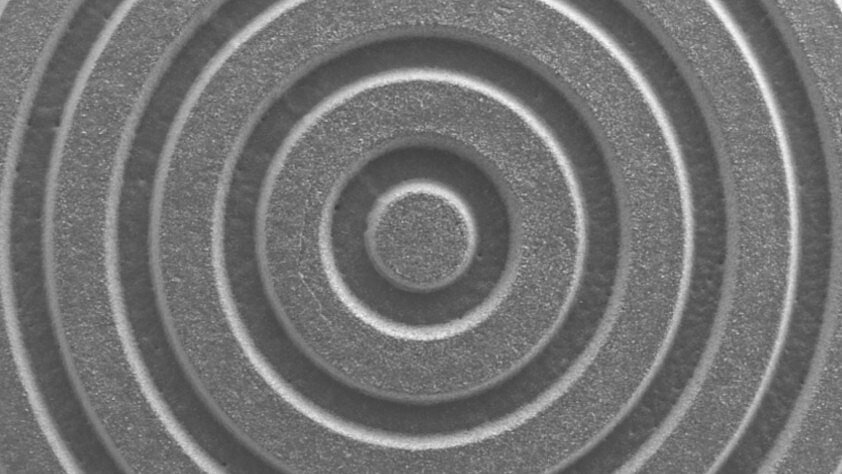
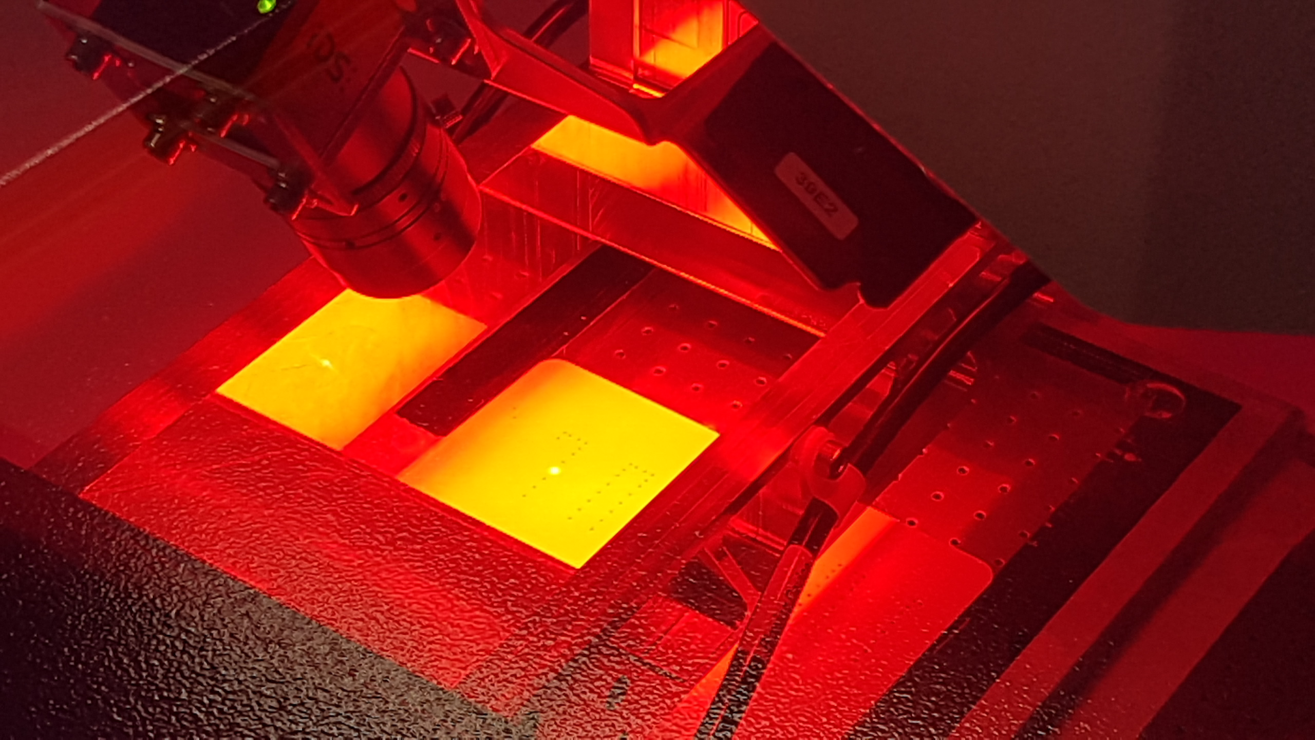
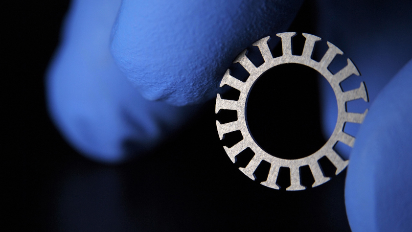
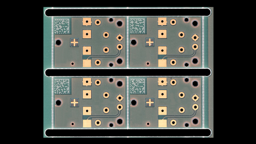
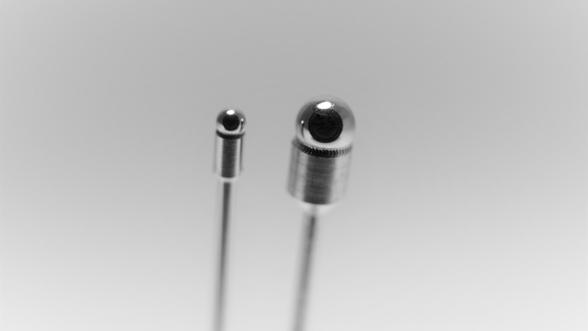
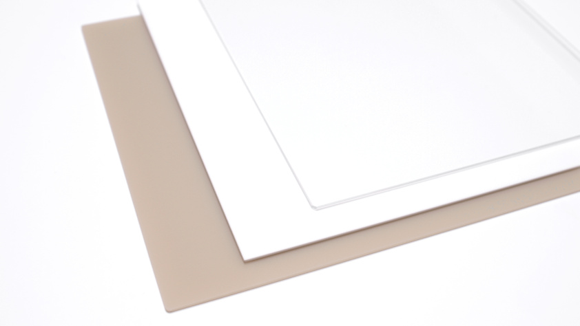
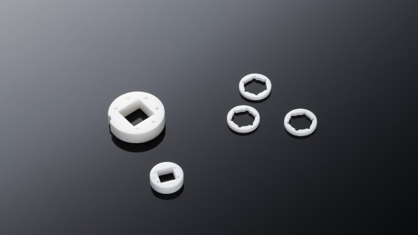
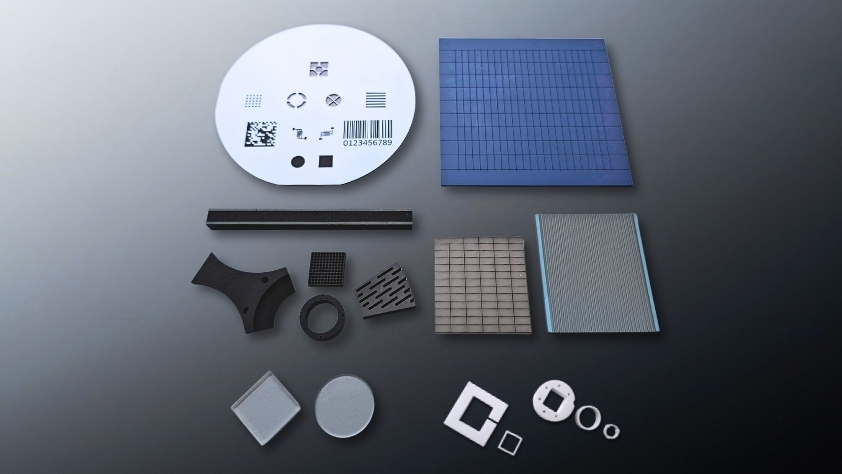
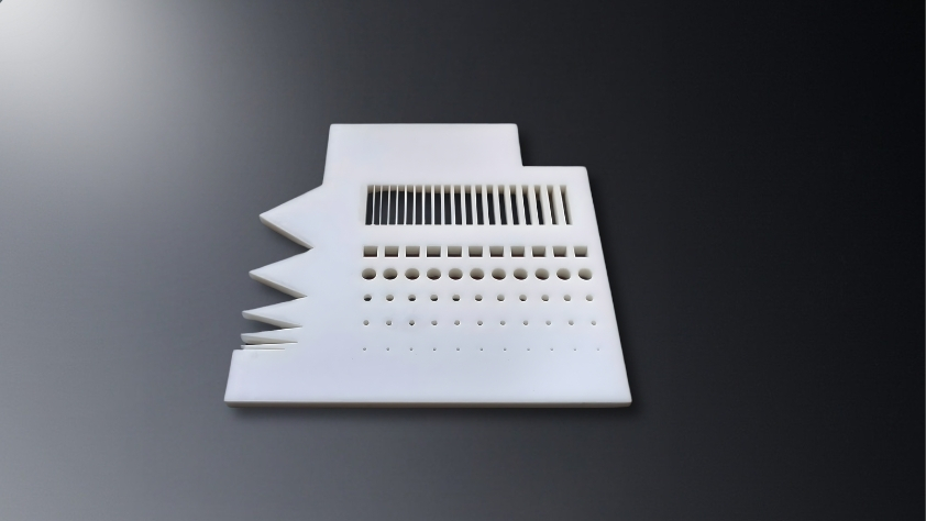
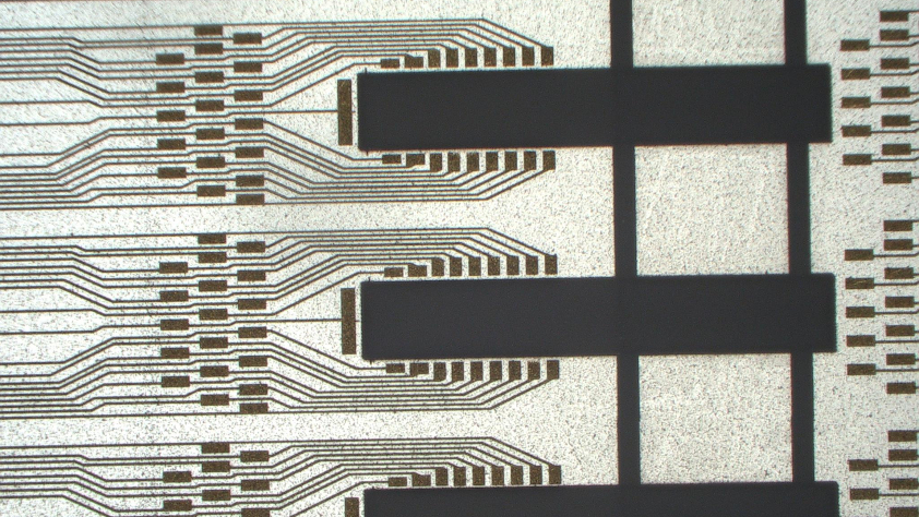
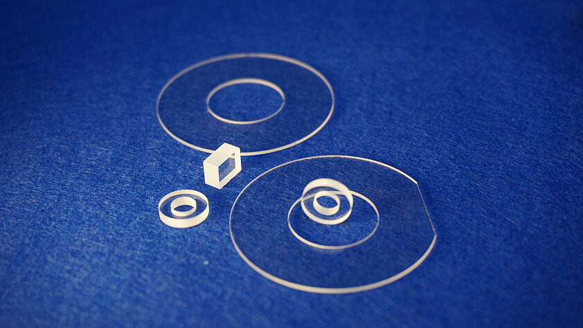
High-performance ceramics such as silicon carbide (SiC) and silicon nitride (SiN) and similar materials are ideal for applications in the semiconductor industry, such as wafer handling, due to their high fracture toughness and low thermal expansion. At the same time, however, their very high hardness and strength place extreme demands on the machining of these materials, with mechanical machining quickly reaching its limits. Laser material processing offers a solution here.
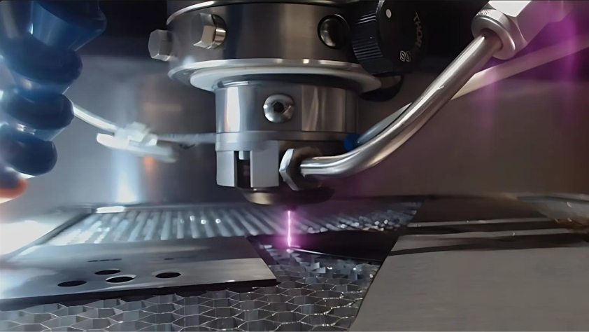
In our latest technical article, “When hardness meets precision: Innovative machining of technical ceramics for semiconductor manufacturing” in Ceramic Applications, issue 01/2026, we show how water-jet guided laser machining enables precise, low-wear, and reliable solutions.
→ Read the full article and discover how new laser technology is opening up entirely new approaches to machining high-performance ceramics!

























![[Translate to English:] Silizium Wafer](/fileadmin/_processed_/4/5/csm_silizium_wafer_842_aca3d0cb65.jpg)