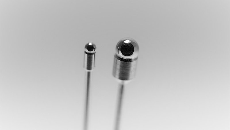
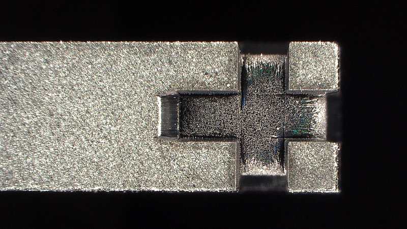
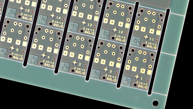
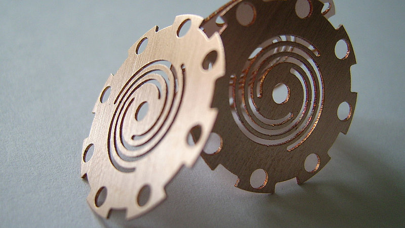
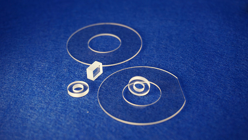
Hard-brittle materials such as high-performance ceramics made of Al2O3, AlN, ZrO, SiN, SiC and LTTC, silicon and semiconductor substrates as well as glass wafers made of materials such as Borofloat® 33, D 263® T eco, AF 32®, AS87®, MEMpax®, BK7 as well as quartz glass are very sensitive to breakage and cracking due to their material compounds.
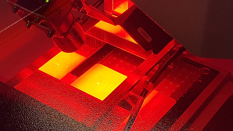
LCP Laser-Cut-Processing GmbH uses the latest ultra-short pulse (USP) laser technology for processing such highly sensitive materials, which has clear advantages over conventional thermal laser processing. This is because the use of USP technology with very short but high pulse frequencies means that there is no heat input into the material. The athermal process thus enables stress-free processing of the material, so that no stress or microcracks occur. As a result, even more filigree structures can be implemented, even thinner materials can be processed, and customer requirements for better miniaturization can be met. Another advantage of USP laser processing is the significantly smaller track width when processing the material, which is reflected positively in a larger area utilization and thus a higher degree of area utilization. USP laser processing also exhibits extremely low to no contamination of the material surface after processing. The technological process with ultra-short pulses prevents any melting or burr formation, so that the cleaning effort is significantly minimized. This is particularly advantageous when processing already printed, coated or assembled payload substrates and wafers. In addition, USP technology offers a wider range of materials and material composites, composites and multilayers that can still be processed with the best results due to their sensitive and very different material properties.
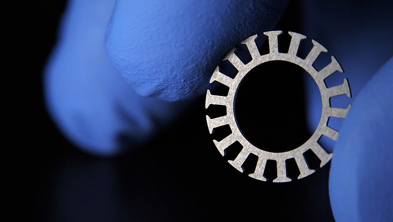
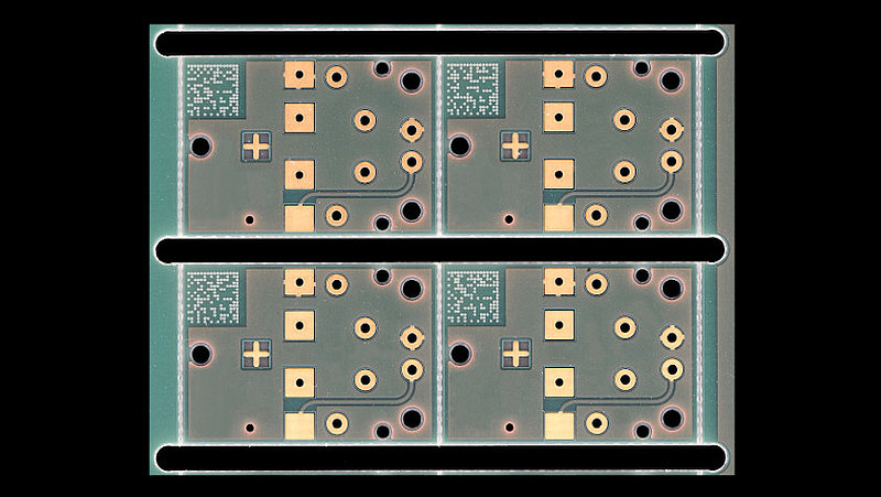
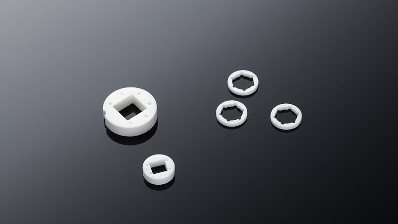
This makes USP laser processing significantly more flexible and also more versatile than other laser technologies. Combined with many years of experience and know-how in the application of special materials, small components and parts with filigree structures of the best processing quality are created. From prototypes to mass production, these laser-machined elements serve as circuit carriers for complex electronics, chip resistors, high-current circuit boards for power electronics, housings for special sensors and interposers, or as manufacturing tools in the form of masks, templates and carriers.
LCP Laser-Cut-Processing GmbH masters precisely this interplay between technology and application know-how in laser fine machining and, as the application center and longstanding experience provider, offers high-end micro-material processing of special materials such as hard-brittle ceramic substrates. In addition to the innovative USP technology, the company also uses other laser technologies that are always at the latest technology level. Outsource your challenges in micro material processing to the specialist. In this way, you remain flexible, can focus on your core competencies and save on your own costly and maintenance-intensive plant technology, tied-up personnel resources and many years of building up in-depth know-how. Your advantage with LCP: You receive a fast, reliable special service adapted to your individual needs, on which you can rely - from consulting and prototype production to possible series production along the entire process chain!
![[Translate to English:] Nutzensubstrat Keramik](/fileadmin/_processed_/9/c/csm_nutzensubstrat_keramik_700_183473a41c.jpg)
![[Translate to English:] Silizium Wafer](/fileadmin/_processed_/8/c/csm_si_wafer_700_2f772abb2c.jpg)
![[Translate to English:] Bauteilverband Keramik](/fileadmin/_processed_/8/a/csm_bauteilverband_keramik_700_155fc5e816.jpg)
![[Translate to English:] Keramikgitter](/fileadmin/_processed_/f/f/csm_keramikgitter_700_a7fc50e7e4.jpg)

![[Translate to English:] LTCC-Substrat](/fileadmin/_processed_/0/1/csm_ltcc_substrat_700_2bb7d7f2c9.jpg)
![[Translate to English:] AlN-Einzelbauteile](/fileadmin/_processed_/5/b/csm_aln_einzelbauteile_700_2f5601ef5e.jpg)


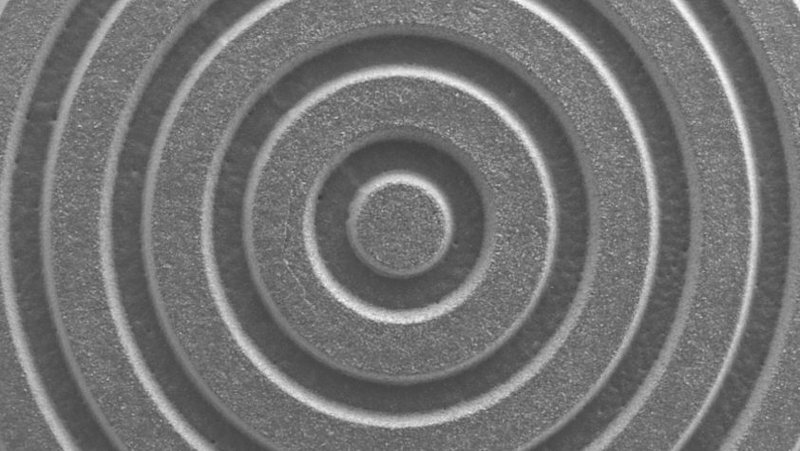
![[Translate to English:] Silizium Wafer](/fileadmin/_processed_/4/5/csm_silizium_wafer_842_022e209b94.jpg)